Backend (Physical Design)
Most companies and people start physical design flow from synthesis , but here I am going to start the flow from data setup and floorplan.
Physical design flow consists of a series of steps as shown below.

This is going to be a series of step-by-step explanation of physical
design flow for the novice. I am going to list out the stages from
Netlist-GDS in this session. Of course some say synthesis should also be
part of physical design, but we will skip that for now.
So, you have completed your RTL, synthesised it and now you have a
netlist & constraints. Next comes the physical design part of
it;making your design into a representation of the actual geometries you
will manufacture. You will do a bunch of stuff here, like floorplanning, placement, CTS,
routing, timing closure, physical verification, formal verification etc.
The major stages are explained below.
I. Netlist In(Init design)
The first stage in physical design flow is reading in the netlist and the constraints to your tool of choice. Let us see what kinds of files we are dealing with here. I have used both Cadence and Synopsys tools extensively, so those are what I will base my examples on. However, every tool uses pretty much the same flow and even the same format files.
-
Gate Level Netlist
Once you choose a process and a library, a synthesis tool will translate your RTL into a collection of interconnected logic gates that define the logic. The most common format is verilog. I had seen some VHDL and EDIF designs when I started my career, but I have only really worked with Verilog files. - Standard Cell Library
In digital design, you have a ready made standard cell library which will be used for synthesis and subsequent layouts. Your netlist will have instantiation of these cells. For digital layout, you need layout and timing abstracts for these cells.
- Layout Model – An abstract model of the standard cell layout is used instead of the complete layout. This will have PINs defined, so as to facilitate automatic routing by the tool as per your netlist. Synopsys tool ICCompiler use “FRAM” views as a PnR abstract. FRAM view is a cell view that has only the PINs and metal and via blockages defined. This makes sure that the interconnection between the PINs can be routed automatically and that the routing tool will not route over existing metal/via areas thus ruling out any shorts. Cadence EDI tools use LEF views, which again has only the PINs and Obstructions (blockages) defined. LEF is an ascii file, so go ahead and have a read.
- Timing Model – Tools also need a timing model in the form of a .lib file. ICC takes a .db file, which is generated from a .lib. This liberty format file will have timing numbers for the various arcs in a cell, generally in a look up model. Please note that .libs may also have cell power information.
- Technology File
The rules pertaining to the process you have selected should also be given to the PnR tool. This includes metal widths, spacing, via definitions etc. ICC takes a milkyway techfile format, while EDI tools take a technology LEF file. - Timing Constraints
SDC files define the timing constraints of your design. You will have the clock definitions, false paths, any input and output delay constraints etc.This is a flow related to synopsys IC Compiler.(commands)
set search_path "<.db_file_paths>"set link_library "* std_lib1.db std_lib2.db"create_mw_lib my_design_lib \-technology <milkyway_techfile> \-mw_reference_library "<milkyway_lib1 milkyway_lib2> \-openread_verilog ./my_design.vcurrent_design <top_module_name>linkread_sdc <sdc_file>The above snippet of code creates a library with the name “my_design_lib”. The .db files are specified using “set link_library” and the paths where they can be found at “set search_path”.
A sample design is shown in below figure (this figure represents data setup i.e design is loaded with all inputs required.)

Until here only data is setup but floorplan, powerplan and pin placement has to be done. Mostly those will be provided by hierarchical people.
Floorplanning
This is the first major step in getting your layout done, and for me this is the most important one.Your floorplan determines your chip quality.At this step, you define the size of your chip/block, allocates power routing resources, place the hard macros, and reserve space for standard cells.Every subsequent stage like placement, routing and timing closure is dependent on how good your foorplan is. In a real time design, you go through many iterations before you arrive at an optimum floorplan.
1. Core Boundary
Floorplan defines the size and shape of your chip/block. A top level digital design will have a rectangular/square shape, whereas a sub block may have rectangular or rectilinear shapes. Core boundary refers to the area where you will be placing standard cells and other IP blocks. You may have power routing spaces allocated outside the core boundary. For a full chip, you will also have IO buffers and IO pads placed outside the core boundary.
In your PnR tool, floorplanning can be controlled by various parameters:
- Aspect ratio: This is the ratio of height divided by width and determines whether you get a square or rectangular floorplan. An aspect ratio of 1 gives you a square floorplan.
- Core utilization
Core utilization = (standard cell area+ macro cells area)/ total core area
A core utilization of 0.8 means that 80% of the area is available for placement of cells, whereas 20% is left free for routing. - Boundary: You can specify a boundary and ask the tool to honour it. This can come in handy when you have an existing boundary from a previous version.When you specify Boundary as the control parameter, both aspect ratio and core utilization are irrelevant. The tool gives you a report of the utilization for the current boundary specified.
- 2. IO Placement/Pin placementread_pin_pad_physical_constraints ./pins.tdfset_fp_pin_constraints -hard_constraints {layer location} -block_levelread_def ./boundary.defcreate_floorplan -control_type boundary -start_first_row -flip_first_row \-left_io2core 10 -bottom_io2core 10 \-right_io2core 10 -top_io2core 10
If you are doing a digital-top design, you need to place IO pads and IO buffers of the chip.Take a reactangular or square chip that has pads in four sides.To start with, you may get the sides and relative positions of the PADs from the designers. You will also get a maximum and minimum die size according to the package you have selected. To place IOs, I use a perl script to place them once I decide on my chip size. If you are doing a digital block, you will need to place pins around the boundary to connect to the higher level routing. Cadence tools can use a DEF file or a custom floorplan file to do this. ICC can read in a DEF or a pin placement file to do the SAME.
DEF extract:
DESIGN my_design_lib;

UNIT DISTANCE MICRON 1000 ;

DIEAREA ( 0 0 ) ( 1914800 1150100 ) ;
PINS 550 ;

- sel[1] + NET sel[1]

  + DIRECTION INOUT

  + LAYER MET3 ( 0 0 ) ( 500 500 )

  + PLACED ( 0 265900 ) N ;

....

END PINS;
END DESIGN;
Macro placement
Once you have the size & shape of the floorplan ready and initialized the floorplan, thereby creating standard cell rows, you are now ready to hand place your macros. Do not use any auto placement, I have not seen anything that works. Flylines in your tool will show you the connection between the macros and standard cells or IOs.
- Use flylines and make sure you place blocks that connects to each other closer
- For a full-chip, if hard macros connect to IOs, place them near the respective IOs
- Consider the power straps while placing macros. You can club macros/memories
-
Creating Power Rings and Straps
This is a topic worthy of its own article, and I will get to arriving
at the number and width of power rings&straps at another post. Let
me just now touch upon how to generate the power rings using ICCompiler.
At this stage, you decide on the trunks that supply power to the core. You also have to make sure that all the hard macros have sufficient rings/straps around it to hook into the PG trunks. As usual, a robust power structure will take iterations and IR drop analysis at a later stage, but a close approximation can be arrived at the initial stages.
create_rectangular_rings, create_rectilinear_rings and create_power_strapsare some commands in ICCompiler that will let you create the power network. - Priority of macro placement is as follows.
2. macros talking to each other
3. macros talking to core(standard cells) .
Placing the Macros inside the core area i.e.,the floor-planning. During the floor-planning we have to follow the steps and techniques to come up with a good floor-plan
• Kept the Macros which are communicating with same type of the Macros close together with the help of fly lines,Colour by hierarchy and data flow diagram.
• Avoided the placement of Macros in front of ports.
• Arranged the Macros to get contiguous core area .
• Reduce the narrow channels between the Macros and provided proper placement.
• Placed the Macros with pins towards the core
II.PLACEMENT
After you have done floorplanning, i.e. created the core area, placed the macros, and decided the power network structure of your design, it is time to let the tool to do standard cell placement. The tool determines the location of each of the components (in digital design, standard cell instantiations) on the die. Various factors come into play, like the timing requirement of the system, the interconnect lengths and hence the connections between cells, power dissipation etc. The interconnect lengths depend on the placement solution used, and it is very important in determining the performance of the system as the geometries shrink.Placement also determines the routability of your design.Placement does not just place the standard cells available in the synthesized netlist. It also optimizes the design, thereby removing any timing violations created due to the relative placement on die.From a user perspective, these are the things important in placement.
After PNS (power Network synthesis the design looks like below.

-
High fanout net synthesis
High fanout nets other than clocks are synthesized at the placement stage. In logic synthesis, high fanout nets like reset, scan enable etc are not synthesized. You should verify that the SDC used for PnR should not have anyset_ideal_networkorset_dont_touchcommands on these signals. Also, make sure you set an appropriate fanout limit for your library using the commandset_max_fanout. e.g.set_max_fanout 20 [current_design]
If a driver has too many loads, it will negatively affect the delay numbers and transitions values. After placement, look for any fanout violations in the timing report. - Use Ideal clock
You are going to synthesize your clock later in the design. So make sure you define the clocks as ideal. If you don’t, HFN synthesis will be done on the clock. Clock constraints like skew or clock buffers are not used, and effectively your clock tree is messed up. In IC Compiler, you can use the following command to make sure clock is not propagated.
set_ideal_network [all_fanout -flat -clock_tree] - Control Congestion
Congestion needs to be analysed after placement and the routing results depend on how congested your design is. Routing congestion may be localised. Some of the things that you can do to make sure routing is hassle free are:- Macro-padding: Macro padding or placement halos around the macros are placement blockages around the edge of the macros. This makes sure that no standard cells are placed near the pin outs of the macros, thereby giving extra breathing space for the macro pin connections to standard cells.
- Maximum Utilization constraint: Some tools let you specify
maximum core utilization numbers for specific regions. If any region has
routing congestion, utilization there can be reduced, thus freeing up
more area for routing.
set_congestion_options -max_util .6 -coordinate {837 114 1103 918} - Placement blockages: The utilization constraint is not a hard rule, and if you want to specifically avoid placement in certain areas, use placement blockages.
- Scan chain reordering
In a less complex design, you don’t usually do scan reordering. However, sometimes it may become difficult to pass scan timing constraints once the placement is done. The scan flip flop placements may create lengthier routes if the consective flops in scan chain are placed far apart due to a functional requirement. In this case, the PnR tool can
reconnect the scan chains, to make routing easier. A prerequisite for this option is a scan DEF for the tool to recognise the chains. - TIE cells
In your netlist, some unused inputs are tied to either VDD/VSS (or logic1/logic0). It is not recommended to connect a gate directly to the power network, so you can use TIEHI or TIELO cells if available in your library for the same. These are single pin cells which effectively ties the pin it connects high or low. After placement, dump out a netlist and serach for direct pin connections to the PG rails (other than power pins). There shouldn’t be any if you are using tie cells. In IC Compiler, use the following commands to connect tie cells.
set getTiePins [get_pins -of [get_nets -all -hier {VDD VSS}]]connect_tie_cells -objects $getTiePins -obj_type port_inst \-tie_high_lib_cell TIEHIX1 -tie_low_lib_cell TIELOX1 -max_fanout 1- TIE cells insertion flows differ slightly between tools, so go through the help.
- Timing
Your clock is not propagated, hence you have a zero skew at this point. Your timing reports should look pretty good. Make sure fanout constraints are met.
check_legality

report_placement_utilization

report_level_shifters -verbose
After placement

Middle shows the standard cell placement which is core logic.
For synchronized designs, data transfer between functional elements are synchronized by clock signals. In a top level digital design, you will have one more more clock sources, like PLLs or oscillators within the chip. You may also have an external clock source connection through an IO. For a digital only block, you will have a clock pin that will be the clock source for the block in question. Clock balancing is important for meeting the design constraints and clock tree synthesis is done after placement to achieve the performance goals.After placement you have positions of all the cells, including macros and standard cells. However, you still have an ideal clock. (For simplicity, we will assume that we are dealing with a single clock for the whole design). At this stage, buffer insertion and gate sizing and any other optimization technique is employed on the data paths, but no change is done to the clock net.The same clock net connects all the synchronous elements in the design, irrespective of the number.This is how your design’s clock network is at this point.
clock net before CTSThis is definitely not something we want. Think just about the load of one clock net. No driver can drive that many flops! But when it is a synchronising signal like clock, load or fanout is not the only thing we are worried about. We also want a “balanced” tree, that is the skew value for the clock tree should be zero. After clock tree synthesis, the clock net will be buffered as below.
Clock Net After CTS.The main concerns in CTS are:Skew – One of the major goals of CTS is to reduce clock skew.
Let us see some definitions before we go into clock skew.Clock SourceClock sources may be external or internal to your chip/block. But for CTS, what we are concerned about is the point from where the clock propagation starts for the digital circuitry. The can be a IO port, outputs or PLL,Oscillators, or even the outputs of a gate down the line. (e.g a mux output).A clock source for CTS may also be specified using ‘create_generated_clock’ command. This defines an internally generated clock for which you want to build a separate tree, with it’s own skew, timing and inter-clock relations.You specify the clock source(s), using the command create_clock.create_clock -name XTALCLK -period 100 -waveform { 0 50 } [get_pins {xtal_inst/OUT}]create_clock -name clk -period 100 -waveform { 0 50 } [get_ports {clk}]create_generated_clock -name div_clk1 \-source [get_pins {block1/clk_out}] -divide_by 2 \-master_clock [get_clocks {clk}]- Clock Sinks
Sinks or clock stop points are nodes which receive the clock. Default sinks are the clock pins of your synchronous elements like Flipflops.
In the picture above, the delay to clock sinks are given. The skew in this case is the difference between the maximum delay and minimum delay.
Skew = 20ns-5ns = 15ns
The goal of clock tree synthesis is to get the skew in the design to be close to zero. i.e. every clock sink should get the clock at the same time.- Clock Sinks
-
Power – Clock is a major power consumer in your design. Clock power
consumption depends on switching activity and wire length. Switching
activity is high, since clock toggles constantly. Clock gating is a
common technique for reducing clock power by shutting off the clock to
unused sinks. Clock gating per se is not done in layout; it should be
incorporated in the design. However,lock tree synthesis tools can
recognise the clock gates, and also do a power aware CTS.
- In the picture above, FF1 gets the ungated clock CLK, and FF2 and any subsequent flop gets a gated clock. This clock is turned on only when the signal EN is present. (See ICG cells).
Make sure that you specify the clock as propagated at CTS stage. i.e. instead of ideal delay for clock, you are now calculating the actual delay value for the clock. This will in turn give you a more realistic report of the timing of the design. You can propagate the clock using the commandset_propgated_clock [all_clocks]


After CTS, the routing process determines the precise paths for
interconnections. This includes the standard cell and macro pins, the
pins on the block boundary or pads at the chip boundary. After placement
and CTS,the tool has information about the exact locations of blocks,
pins of blocks, and I/O pads at chip boundaries. The logical
connectivity as defined by the netlist is also available to the tool. In
routing stage, metal and vias are used to create the electrical
connection in layout so as to complete all connections defined by the
netlist. Now, to do the actual interconnections, the tool relies on some
“Design Rules”. It is essential that
- Tool completes all connections that are defined by the netlist (100% routability), i.e. no LVS errors.
- No design rules are violated in completing the routes(No DRC errors).
- All timing constraints are met.
Process Design Rules
If you refer to Physical Design Flow I,
an input to the PnR tool is a ‘Technology File’ (or technology LEF for
Cadence.) These are the constraints that the router should honour.
An example for technology file rules for metal1 & via1 are given below.
Layer "M1" {
layerNumber = 10
maskName = "metal1"
pitch = 0.56
defaultWidth = 0.24
minWidth = 0.24
minSpacing = 0.24
fatWireThreshold = 10
}
Layer "VIA1" {
layerNumber = 11
maskName = "via1"
pitch = 0
defaultWidth = 0.24
minWidth = 0.24
minSpacing = 0.24
}
ContactCode "via1" {
contactCodeNumber = 1
cutLayer = "VIA1"
lowerLayer = "M1"
upperLayer = "M2"
isDefaultContact = 1
cutWidth = 0.24
cutHeight = 0.24
upperLayerEncWidth = 0.01
upperLayerEncHeight = 0.06
lowerLayerEncWidth = 0.06
lowerLayerEncHeight = 0.01
minCutSpacing = 0.24
}
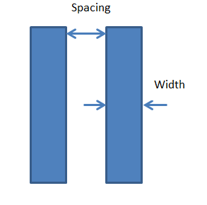
Your techfile will have many more parameters for each layer. As you can
see, for M1 above, minimum spacing, minimum width, minimum area etc are
defined. It also specifies which via connects the two metal layers M1
& M2. If any of these parameters like spacing, width, via size etc
are violated for any routing the tool does, you will get a DRC error.
Most of the routers available are grid based routers. There are routing grids defined for the entire layout. Consider it like a graph as below. For grid based routers, there are also preferred routing direction defined for each metal layer. e.g. Metal1 has a preferred direction of “horizontal’, metal2 has preferred routing direction of “vertical’ and so on. So, in the whole layout, metal1 routing grids will be drawn (superimposed) horizontally with metal1 wire picth and metal2 grids will be drawn vertically with metal2 wire pitch between each. You can see that the technology section above has a”pitch” defined for metal1.
pitch = 0.56
Routing Grids
The first figure on left figure shows how routing grids are drawn. I
am only considering two metals for now, but in a process with more
metals, similar grids will be superimposed on the layout for all
available metals. Pitch is calculated by determining
the minimum spacing required between grid lines of same metal. This can
be the minimum spacing of the metal itself, but is usually a value
greater than the minimum spacing. This is calculated by taking into
account the via dimension as well, so that no two adjacent wires on the
grid create any DRC violation even when there are vias present.
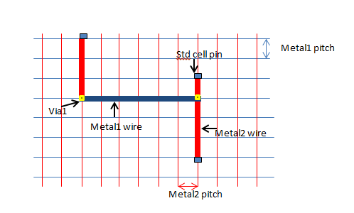
Grid based routing with two metals
In a grid based routing algorithm, the router switches the metal as per preferred direction to interconnect the nodes. As you can see in the second figure, metal1 & metal2 wires are drawn along the metal1 & metal2 grids respectively. They are interconnected by via1 to complete the routing path.
Let’s see some more routing related terms.
Global & Detail Routing
The PnR tools you use may let you do routing in various stages, like
global routing, track assignment and detailed routing. It could also be
that all these algorithmic stages are masked from you and you just have a
couple of commands to play with. Most PnR tools deal with the routing
problem in a two stage approach. In global routing, the tool partitions
the design into routing regions. A rough route is determined taking into
account the number of tracks available in each region. Routing
congestion is also determined at this stage by calculating 1) how many
nets should pass through the region; 2) How many routing tracks are
available in the region. In detailed routing, global routing results are
used to lay the actual wires interconnecting the nodes. Do a man on the
routing options command and you can see how much controllability is
available to you in each of these stages for the tool of your choice.
Routing Congestion
It is difficult to route a highly congested design. Some not-so
congested designs may have pockets of high congestion which will again
create routing issues. It is important that the congestion is analysed
and fixed before detailed routing. After CTS, the tool can give you a
congestion map by a trial route/ global route values. There are commands
to check routability which gives you congestion numbers, blocked pins
etc, like
check_routability.
Routing Order
It is recommended that you route sensitive nets like clock before the
rest of the signal route. My assumption is that you have completed
power routing after the floorplan stage( because that is what I do.).
For this discussion I am going with a traditional routing approach and
not considering signal integrity issues. Anyway the order of routing is:
- Power routing : Connect the macro and standard cell power pins to the power rings and staps you have created for the design. IR drop
- Clock Routing : We do not want to upset the skew and delay values for the clock net as much as possible. So the clocks are given higher priority in using routing resources and routed prior to any other net routing. Clock routing can be limited to higher metal layers for reduced RC numbers.
- Signal Routing : The rest of the nets are routed. We can also route groups of nets, and non-default routing rules can also be applied to select nets.
An Example: ICCompiler Script for Routing
################ Power Routing ############################
preroute_standard_cells -connect horizontal -do_not_route_over_macros
verify_pg_nets
################ Clock Routing ############################
set_parameter -module droute -name doAntennaConx -value 4
source -e $ant_rul_file
set_route_options \
-groute_skew_control true \
-groute_clock_routing balanced \
-droute_CTS_nets normal \
-same_net_notch check_and_fix \
-fat_wire_check merge_then_check \
-merge_fat_wire_on preroute_signal \
-fat_blockage_as fat_wire
set_route_zrt_common_options -concurrent_redundant_via_mode insert_at_high_cost
route_zrt_clock_tree
################ Signal Routing############################
set_route_zrt_detail_options -port_antenna_mode jump
check_routeability
route_opt

See the ant_rule_file that is sourced into the tool?
Antenna Violations and rules will be explained in the next article.
Signal Integrity, EM rules, Antenna and reliability rules, Post Route
optimizations etc also are important in today’s designs to meet design
and manufacturing objectives. However, this is a pretty good starting
point to start tackling each of these aspects one by one.
After routing, your layout is complete. Now a number of checks are performed to verify that the drawn layout works as intended.
- Physical verification
- Equivalence Checking
- Timing Analysis
Equivalence check will compare the netlist we started out with
(pre-layout/synthesis netlist) to the netlist written out by the tool
after PnR(postlayout netlist). Physical verification will verify that the
post-layout netlist and the layout are equivalent. i.e. all connections
specified in the netlist is present in the layout.This article explains
physical verification.
After routing, your PnR tool should give you zero DRC/LVS violations.
However, the PnR tool deals with abstracts like FRAM or LEF views. We
use dedicated physical verification tools for signoff LVS and DRC
checks. Some of these are Hercules from Synopsys, Assura from Cadence
and Calibre from MentorGraphics.
The major checks are:
- DRCDRC checks determine if the layout satisfies a set of rules required for manufacturing. The most common of these are spacing rules between metals, minimum width rules, via rules etc.There will also be specific rules pertaining to your technology. An input to the design rule tool is a ‘design rule file’ (called a runset by Synopsys’ hercules). The design rules ensure sufficient margins to correctly define the geometries without any connectivity issues due to proximity in the semiconductor manufacturing processes, so as to ensure that most of the parts work correctly. The minumum width rules exists for all mask layers, and spacing between the same layers are also specified. Spacing rules may change depending on the width of one or both of the layers as well. There can also be rules between two different layers, and specific via density rules etc. If the design rules are violated, the chip may not be functional.
DRC – Spacing & Width checksDRC checking software, like Assura, Hercules or Calibre usually takes the layout in any of the supported formats, like GDSII. - LVS
LVS is another major check in the physical verification stage. Here you are verifying that the layout you have created is functionally the same as the schematic/netlist of the design-that you have correctly transferred into geometries your intent while creating the design. So all the connections should be proper and there shouldn’t any missing connections etc.The LVS tool creates a layout netlist, by extracting the geometries. This layout netlist is compared with the schematic netlist. The tool may require some steps to create either of these netlists(e.g. nettran run in synopsys)
If the two netlists match, we get an LVS clean result. Else the tool reports the mismatch and the component and location of the mismatch. Along with formal verification, which verifies if your pre-layout netlist matches the post-layout netlist,LVS verifies the correctness of the layout w.r.t intended functionality.Some of the LVS errors are:- Shorts – Wires that should not be connected are overlapping.
- Opens – Connections are not complete for certain nets.
- Parameter mismatch – LVS also checks for parameter mismatches. e.g. It may match a resistor in both layout and schematic, but the resistor values may be different. This will be reported as a parameter mismatch.
- Unbound pins – If the pins don’t have a geometry, but all the connection to the net are made, and unbound pin is reported.
- Antenna
- ERCERC (Electrical rule check) involves checking a design for all electrical connections that are considered dangerous.
- Floating gate error – If any gate is unconnected, this could lead to leakage issues.
- VDD/VSS errors – The well geometries need to be connected to power/Ground and if the PG connection is not complete or if the pins are not defined, the whole layout can report errors like “NWELL not connected to VDD.
Process antenna effect or “plasma induced gate oxide damage” is a
manufacturing effect. i.e. this is a type of failure that can occur
solely at the manufacturing stage. This is a gate damage that can occur
due to charge accumulation on metals and discharge to a gate through
gate oxide.
Let us see how this happens. In the manufacturing process, metals are
built layer by layer. i.e. metal1 is deposited first, then all unwanted
portions are etched away, with plasma etching. The metal geometries
when they are exposed to plasma can collect charge from it. Once metal1
is completed, via1 is built, then metal2 and so on. So with each
passing stage, the metal geometries can build up static electricity. The
larger the metal area that is exposed to the plasma, the more charge
they can collect. If the charge collected is large enough to cause
current to flow to the gate, this can cause damage to the gate oxide.
This happens because since the layers are built one-by-one, a
source/drain implant may not be available for discharge as in fig.b.
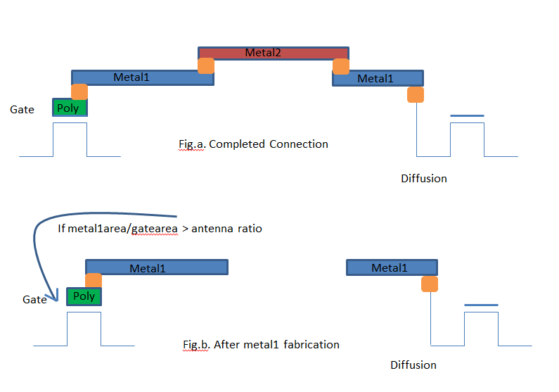
Process Antenna
Antenna rules are normally expressed as an allowable ratio of metal
area to gate area. Each foundry sets a maximum allowable antenna ratio
for its processes. If the metal area–which is cumulative, i.e. the sum
of the ratios of all lower layer interconnects in addition to the layer
in check–is greater than the allowable area, the physical verification
tool flags an error.For example, let’s say maximum allowable antenna
ratio for metal1 is 400. If the gate area is 1 sq.u and if the metal
area connecting to the gate is 500 sq.u, there will be a process antenna
violation.
This comment has been removed by the author.
ReplyDeleteSir , can u provide about global skew and local skew
ReplyDeleteNice Blog. Thanks for sharing
ReplyDeleteExploring the Role of Semiconductors in IoT and Smart Devices
What are the common approaches to ASIC Verification?
The Impact of ASICs on the Evolution of Satellite Technology
Understanding the differences between clock gating and power gating
Understanding the Chip Design Process